-
Part Symbol
-
Footprint
-
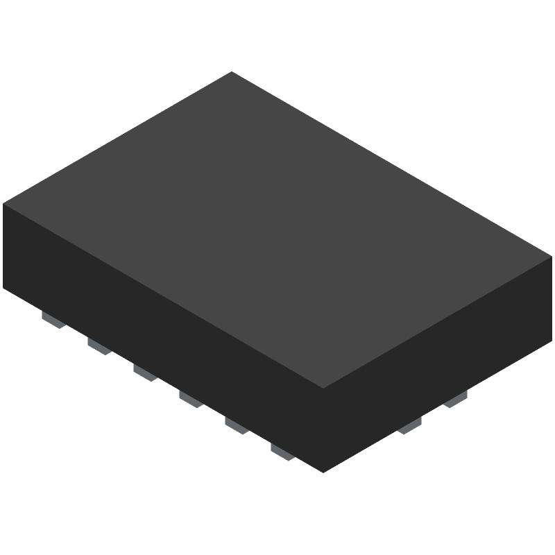
3D Model
Available Download Formats
By downloading CAD models, you agree to our Terms & Conditions and Privacy Policy
Low Voltage Dual Supply 4-Bit Signal Translator with Configurable Voltage Supplies and Signal Levels and 3-STATE Outputs and Independent Direction Controls, WQFN-16, 3000-REEL
Tip: Data for a part may vary between manufacturers. You can filter for manufacturers on the top of the page next to the part image and part number.
FXL4TD245BQX by onsemi is an Other Interface IC.
Other Interface ICs are under the broader part category of Drivers And Interfaces.
A driver controls the current or voltage delivered to components like LCDs or motors, while an interface component connects systems for data transfer and control. Read more about Drivers And Interfaces on our Drivers And Interfaces part category page.
| Part # | Distributor | Description | Stock | Price | Buy | |
|---|---|---|---|---|---|---|
|
DISTI #
61M6452
|
Newark | Fxl Tiny Translator, Smd, Dqfn-16, No. Of Inputs:4, Output Current:24Ma, Propagation Delay:3.5Ns, No. Of Pins:16Pins, Logic Case Style:Dqfn, Supply Voltage Min:1.1V, Supply Voltage Max:3.6V, Operating Temperature Min:-40°C, Operatingrohs Compliant: Yes |Onsemi FXL4TD245BQX RoHS: Compliant Min Qty: 5 Package Multiple: 1 Date Code: 1 Container: Cut Tape | 5685 |
|
$0.2680 / $0.5600 | Buy Now |
|
DISTI #
85AC1849
|
Newark | Low Volt Lvl Translator, -40 To 85Deg C, No. Of Inputs:4, Output Current:-, Propagation Delay:3.5Ns, No. Of Pins:16Pins, Logic Case Style:Dqfn, Supply Voltage Min:1.1V, Supply Voltage Max:3.6V, Operating Temperature Min:-40°C, Rohs Compliant: Yes |Onsemi FXL4TD245BQX RoHS: Compliant Min Qty: 3000 Package Multiple: 1 Date Code: 1 Container: Reel | 0 |
|
$0.2190 / $0.2310 | Buy Now |
|
DISTI #
512-FXL4TD245BQX
|
Mouser Electronics | Translation - Voltage Levels LV Dual Supply 4-Bit Signal Translator RoHS: Compliant | 15344 |
|
$0.2190 / $0.5600 | Buy Now |
|
DISTI #
V72:2272_06339873
|
Arrow Electronics | Voltage Level Translator 4-CH Bidirectional 6-Pin WDFN EP T/R RoHS: Compliant Min Qty: 1 Package Multiple: 1 Lead time: 10 Weeks Date Code: 2347 Container: Cut Strips | Americas - 609 |
|
$0.2352 / $0.3635 | Buy Now |
|
|
Future Electronics | FXL4TD245 Series 3.6 V Low Voltage Dual Supply 4-Bit Signal Translator - DQFN-14 RoHS: Compliant pbFree: Yes Min Qty: 1 Package Multiple: 1 Lead time: 10 Weeks Container: Cut Tape/Mini-Reel | 1500Cut Tape/Mini-Reel |
|
$0.4050 / $0.6500 | Buy Now |
|
|
Future Electronics | FXL4TD245 Series 3.6 V Low Voltage Dual Supply 4-Bit Signal Translator - DQFN-14 RoHS: Compliant pbFree: Yes Min Qty: 3000 Package Multiple: 3000 Lead time: 10 Weeks Container: Reel | 0Reel |
|
$0.2000 / $0.2100 | Buy Now |
|
|
Onlinecomponents.com | Low Voltage Dual Supply 4-Bit Signal Translator with Configurable Voltage Supplies and Signal Levels and 3-STATE Outputs and Independent Direction Controls RoHS: Compliant |
3000 In Stock |
|
$0.2114 / $0.2273 | Buy Now |
|
DISTI #
83629534
|
Verical | Voltage Level Translator 4-CH Bidirectional 6-Pin WDFN EP T/R RoHS: Compliant Min Qty: 3000 Package Multiple: 3000 Date Code: 2423 | Americas - 3000 |
|
$0.2763 / $0.2955 | Buy Now |
|
DISTI #
87892149
|
Verical | Voltage Level Translator 4-CH Bidirectional 6-Pin WDFN EP T/R RoHS: Compliant Min Qty: 45 Package Multiple: 1 Date Code: 2237 | Americas - 1601 |
|
$0.2850 / $0.3260 | Buy Now |
|
DISTI #
74491173
|
Verical | Voltage Level Translator 4-CH Bidirectional 6-Pin WDFN EP T/R RoHS: Compliant Min Qty: 26 Package Multiple: 1 Date Code: 2347 | Americas - 609 |
|
$0.2352 / $0.2886 | Buy Now |
By downloading CAD models, you agree to our Terms & Conditions and Privacy Policy
|
|
FXL4TD245BQX
onsemi
Buy Now
Datasheet
|
Compare Parts:
FXL4TD245BQX
onsemi
Low Voltage Dual Supply 4-Bit Signal Translator with Configurable Voltage Supplies and Signal Levels and 3-STATE Outputs and Independent Direction Controls, WQFN-16, 3000-REEL
|
| Pbfree Code | Yes | |
| Rohs Code | Yes | |
| Part Life Cycle Code | Active | |
| Ihs Manufacturer | ONSEMI | |
| Part Package Code | WQFN-16 | |
| Package Description | DQFN-16 | |
| Manufacturer Package Code | 510CC | |
| Reach Compliance Code | compliant | |
| ECCN Code | EAR99 | |
| HTS Code | 8542.39.00.01 | |
| Factory Lead Time | 10 Weeks | |
| Samacsys Manufacturer | onsemi | |
| Delay-Max | 22 ns | |
| Interface IC Type | VOLTAGE LEVEL TRANSLATOR | |
| JESD-30 Code | R-XQCC-N16 | |
| JESD-609 Code | e4 | |
| Length | 3.5 mm | |
| Moisture Sensitivity Level | 1 | |
| Number of Bits | 4 | |
| Number of Functions | 1 | |
| Number of Terminals | 16 | |
| Operating Temperature-Max | 85 °C | |
| Operating Temperature-Min | -40 °C | |
| Output Characteristics | 3-STATE | |
| Output Latch or Register | NONE | |
| Output Polarity | TRUE | |
| Package Body Material | UNSPECIFIED | |
| Package Code | HVQCCN | |
| Package Equivalence Code | LCC16,.1X.14,20 | |
| Package Shape | RECTANGULAR | |
| Package Style | CHIP CARRIER, HEAT SINK/SLUG, VERY THIN PROFILE | |
| Peak Reflow Temperature (Cel) | 260 | |
| Qualification Status | Not Qualified | |
| Seated Height-Max | 0.8 mm | |
| Supply Current-Max | 100 mA | |
| Supply Voltage-Max | 3.6 V | |
| Supply Voltage-Min | 1.1 V | |
| Supply Voltage-Nom | 1.2 V | |
| Surface Mount | YES | |
| Temperature Grade | INDUSTRIAL | |
| Terminal Finish | Nickel/Palladium/Gold (Ni/Pd/Au) | |
| Terminal Form | NO LEAD | |
| Terminal Pitch | 0.5 mm | |
| Terminal Position | QUAD | |
| Time@Peak Reflow Temperature-Max (s) | 30 | |
| Width | 2.5 mm |
A 2-layer or 4-layer PCB with a solid ground plane and thermal vias is recommended. Ensure a minimum of 1mm clearance around the device for airflow and heat dissipation.
Implement a robust thermal management system, including a heat sink and thermal interface material. Ensure the device is operated within the recommended junction temperature (TJ) range of -40°C to 150°C.
Ensure the input signal rise and fall times are within 10ns to 100ns. The device requires a minimum input pulse width of 10ns and a maximum frequency of 100 MHz.
Implement ESD protection using TVS diodes or ESD arrays on the input and output lines. Ensure the protection devices are rated for the maximum voltage and current of the application.
Power up the device in the following sequence: VCC, then VIN. Ensure a stable 3.3V ±10% supply voltage and a minimum of 1.8V for VIN. Use a low-dropout regulator (LDO) or a switching regulator with a high power supply rejection ratio (PSRR).