-
Part Symbol
-
Footprint
-
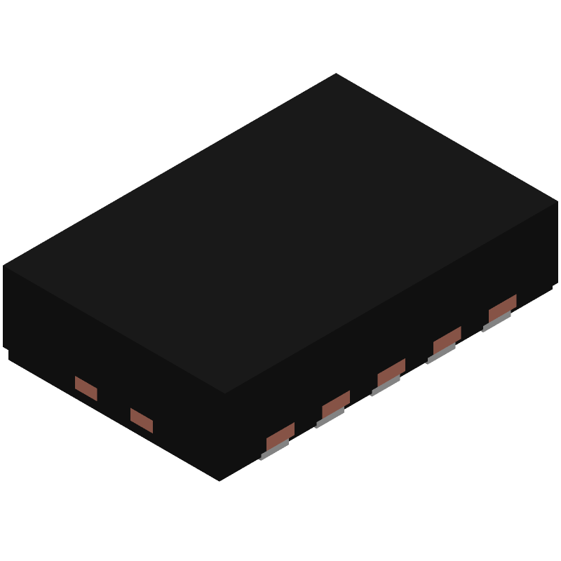
3D Model
Available Download Formats
By downloading CAD models, you agree to our Terms & Conditions and Privacy Policy

Automotive 2-channel 12-bit 140-kSPS I2C-compatible ADC with programmable threshold and host wake-up 10-WSON -40 to 125
Tip: Data for a part may vary between manufacturers. You can filter for manufacturers on the top of the page next to the part image and part number.
ADS7142QDQCRQ1 by Texas Instruments is an Analog to Digital Converter.
Analog to Digital Converters are under the broader part category of Converters.
A converter is an electrical circuit that transforms electric energy into a different form that will support a elecrical load needed by a device. Read more about Converters on our Converters part category page.
| Part # | Distributor | Description | Stock | Price | Buy | |
|---|---|---|---|---|---|---|
|
DISTI #
296-ADS7142QDQCRQ1CT-ND
|
DigiKey | IC ADC 12BIT SAR 10WSON Min Qty: 1 Lead time: 18 Weeks Container: Digi-Reel®, Tape & Reel (TR), Cut Tape (CT) |
10001 In Stock |
|
$1.2138 / $2.5600 | Buy Now |
|
DISTI #
595-ADS7142QDQCRQ1
|
Mouser Electronics | Analog to Digital Converters - ADC Automotive 2-channel 12-bit 140-kSPS I2C RoHS: Compliant | 6230 |
|
$1.2100 / $2.5600 | Buy Now |
|
|
LCSC | 12Bit 1.65V3.6V 140kHz I2C WSON-10-EP(2x3) Analog to Digital Converters (ADC) ROHS | 9 |
|
$2.1384 / $2.2618 | Buy Now |
By downloading CAD models, you agree to our Terms & Conditions and Privacy Policy
|
|
ADS7142QDQCRQ1
Texas Instruments
Buy Now
Datasheet
|
Compare Parts:
ADS7142QDQCRQ1
Texas Instruments
Automotive 2-channel 12-bit 140-kSPS I2C-compatible ADC with programmable threshold and host wake-up 10-WSON -40 to 125
|
| Pbfree Code | Yes | |
| Rohs Code | Yes | |
| Part Life Cycle Code | Active | |
| Ihs Manufacturer | TEXAS INSTRUMENTS INC | |
| Package Description | WSON-10 | |
| Reach Compliance Code | compliant | |
| ECCN Code | EAR99 | |
| HTS Code | 8542.39.00.01 | |
| Date Of Intro | 2019-10-02 | |
| Samacsys Manufacturer | Texas Instruments | |
| Analog Input Voltage-Max | 3.6 V | |
| Analog Input Voltage-Min | ||
| Conversion Time-Max | 1.8 µs | |
| Converter Type | ADC, SUCCESSIVE APPROXIMATION | |
| JESD-30 Code | R-PDSO-N10 | |
| JESD-609 Code | e3 | |
| Length | 3 mm | |
| Linearity Error-Max (EL) | 0.0671% | |
| Moisture Sensitivity Level | 2 | |
| Number of Analog In Channels | 2 | |
| Number of Bits | 12 | |
| Number of Functions | 1 | |
| Number of Terminals | 10 | |
| Operating Temperature-Max | 125 °C | |
| Operating Temperature-Min | -40 °C | |
| Output Bit Code | BINARY | |
| Output Format | SERIAL | |
| Package Body Material | PLASTIC/EPOXY | |
| Package Code | HVSON | |
| Package Equivalence Code | SOLCC10,.08,20 | |
| Package Shape | RECTANGULAR | |
| Package Style | SMALL OUTLINE, HEAT SINK/SLUG, VERY THIN PROFILE | |
| Peak Reflow Temperature (Cel) | 260 | |
| Sample Rate | 0.14 MHz | |
| Screening Level | AEC-Q100 | |
| Seated Height-Max | 0.8 mm | |
| Supply Voltage-Min | 1.65 V | |
| Supply Voltage-Nom | 3 V | |
| Surface Mount | YES | |
| Temperature Grade | AUTOMOTIVE | |
| Terminal Finish | Matte Tin (Sn) | |
| Terminal Form | NO LEAD | |
| Terminal Pitch | 0.5 mm | |
| Terminal Position | DUAL | |
| Time@Peak Reflow Temperature-Max (s) | 30 | |
| Width | 2 mm |
Texas Instruments recommends a 4-layer PCB with a solid ground plane, and to keep the analog and digital signals separate. The datasheet provides a recommended layout and routing guide, but it's also recommended to consult with a PCB design expert to ensure optimal performance.
To optimize the ADC's performance, it's essential to understand the application's requirements and adjust the ADC's settings accordingly. This includes selecting the correct gain, offset, and sampling rate. Additionally, ensuring a clean power supply, minimizing noise, and using proper filtering can also improve performance.
The ADS7142QDQCRQ1 can achieve a maximum sampling rate of 1 MSPS. However, the actual sampling rate may be limited by the system's clock speed, data conversion time, and other factors. It's essential to consult the datasheet and application notes for specific guidance.
The ADS7142QDQCRQ1 has a latency of approximately 1.5 clock cycles. To ensure data integrity, it's essential to consider the ADC's latency when designing the system's timing and synchronization. Additionally, using a FIFO or buffer can help manage data flow and prevent data loss.
The recommended power-up sequence is to power up the analog supply (AVDD) first, followed by the digital supply (DVDD). When powering down, the sequence should be reversed. It's essential to follow the recommended power-up and power-down sequence to prevent damage to the device.