-
Part Symbol
-
Footprint
-
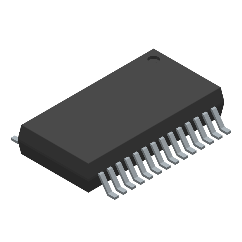
3D Model
Available Download Formats
By downloading CAD models, you agree to our Terms & Conditions and Privacy Policy
4-output Differential Buffer for PCI-Express, SSOP0/Reel
Tip: Data for a part may vary between manufacturers. You can filter for manufacturers on the top of the page next to the part image and part number.
9DB104BFLFT by Renesas Electronics Corporation is a Clock Driver.
Clock Drivers are under the broader part category of Logic Components.
Digital logic governs the behavior of signals in electronic circuits, enabling complex decisions based on simple binary inputs (yes/no). Logic components perform operations from these signals. Read more about Logic Components on our Logic part category page.
| Part # | Distributor | Description | Stock | Price | Buy | |
|---|---|---|---|---|---|---|
|
DISTI #
800-3644-1-ND
|
DigiKey | IC BUFFER 4OUTPUT DIFF 28-SSOP Min Qty: 1 Lead time: 36 Weeks Container: Cut Tape (CT), Tape & Reel (TR) |
516 In Stock |
|
$2.8968 / $4.9400 | Buy Now |
|
|
New Advantage Corporation | PLL Based Clock Driver, 9DB Series, 8 True Output(s), 0 Inverted Output(s), PDSO28 RoHS: Compliant Min Qty: 1 Package Multiple: 1 | 360 |
|
$7.1900 / $7.5900 | Buy Now |
By downloading CAD models, you agree to our Terms & Conditions and Privacy Policy
|
|
9DB104BFLFT
Renesas Electronics Corporation
Buy Now
Datasheet
|
Compare Parts:
9DB104BFLFT
Renesas Electronics Corporation
4-output Differential Buffer for PCI-Express, SSOP0/Reel
|
| Pbfree Code | Yes | |
| Rohs Code | Yes | |
| Part Life Cycle Code | Obsolete | |
| Ihs Manufacturer | RENESAS ELECTRONICS CORP | |
| Part Package Code | SSOP | |
| Package Description | 0.209 INCH, ROHS COMPLIANT, MO-150, SSOP-28 | |
| Pin Count | 28 | |
| Manufacturer Package Code | PYG28 | |
| Reach Compliance Code | compliant | |
| ECCN Code | NLR | |
| HTS Code | 8542390001 | |
| Samacsys Manufacturer | Renesas Electronics | |
| Family | 9DB | |
| Input Conditioning | DIFFERENTIAL | |
| JESD-30 Code | R-PDSO-G28 | |
| JESD-609 Code | e3 | |
| Length | 10.2 mm | |
| Logic IC Type | PLL BASED CLOCK DRIVER | |
| Moisture Sensitivity Level | 1 | |
| Number of Functions | 1 | |
| Number of Inverted Outputs | ||
| Number of Terminals | 28 | |
| Number of True Outputs | 8 | |
| Operating Temperature-Max | 70 °C | |
| Operating Temperature-Min | ||
| Output Characteristics | 3-STATE | |
| Package Body Material | PLASTIC/EPOXY | |
| Package Code | SSOP | |
| Package Equivalence Code | SSOP28,.3 | |
| Package Shape | RECTANGULAR | |
| Package Style | SMALL OUTLINE, SHRINK PITCH | |
| Packing Method | TR | |
| Peak Reflow Temperature (Cel) | 260 | |
| Qualification Status | Not Qualified | |
| Same Edge Skew-Max (tskwd) | 0.05 ns | |
| Seated Height-Max | 2 mm | |
| Supply Voltage-Max (Vsup) | 3.465 V | |
| Supply Voltage-Min (Vsup) | 3.135 V | |
| Supply Voltage-Nom (Vsup) | 3.3 V | |
| Surface Mount | YES | |
| Temperature Grade | COMMERCIAL | |
| Terminal Finish | MATTE TIN | |
| Terminal Form | GULL WING | |
| Terminal Pitch | 0.65 mm | |
| Terminal Position | DUAL | |
| Time@Peak Reflow Temperature-Max (s) | 30 | |
| Width | 5.3 mm |
The recommended operating temperature range for the 9DB104BFLFT is -40°C to 125°C.
To ensure reliable data transfer, ensure that the clock frequency is within the recommended range, and use a stable clock source. Also, ensure that the data lines are properly terminated and that the signal integrity is maintained.
The maximum clock frequency supported by the 9DB104BFLFT is 100 MHz.
Follow the recommended power-up and power-down sequencing in the datasheet to ensure proper device operation. Typically, the power supply voltage (VCC) should be applied before the clock signal, and the clock signal should be stable before applying the input signals.
Follow good PCB layout and routing practices, such as keeping signal traces short and away from noise sources, using ground planes, and avoiding vias under the device. Also, ensure that the device is properly decoupled and that the power supply is clean and stable.