-
Part Symbol
-
Footprint
-
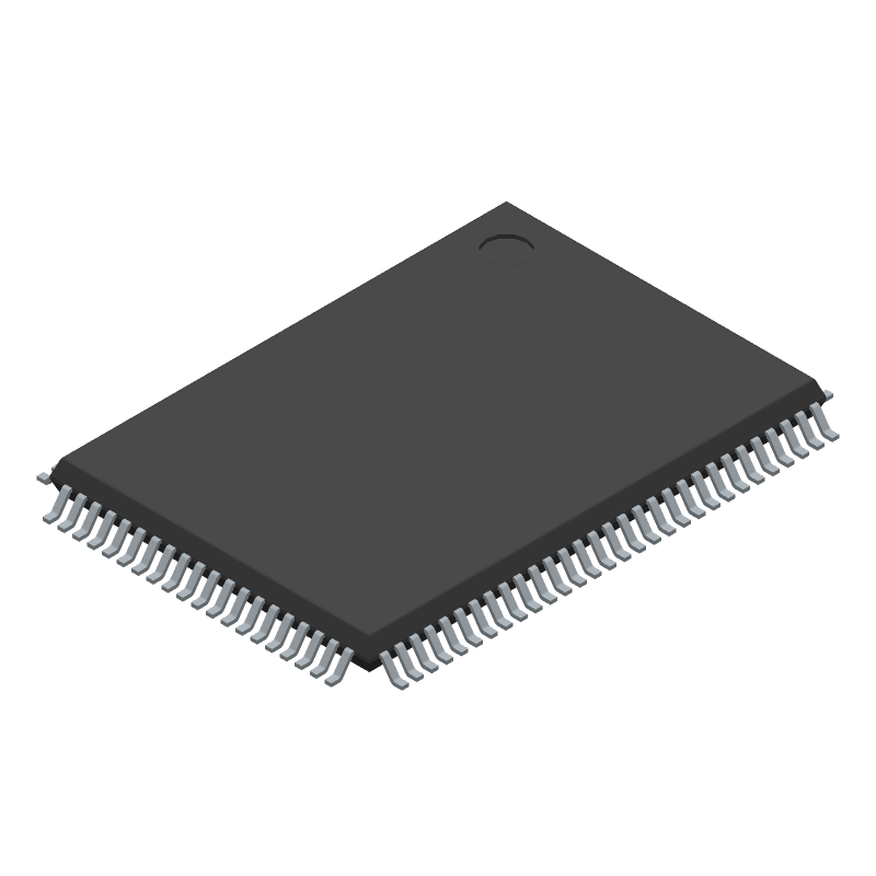
3D Model
Available Download Formats
By downloading CAD models, you agree to our Terms & Conditions and Privacy Policy
2 Channel T1 / J1 / E1 Transceiver, TQFP72/Tray
Tip: Data for a part may vary between manufacturers. You can filter for manufacturers on the top of the page next to the part image and part number.
82P2282PFG by Renesas Electronics Corporation is a Digital Transmission Interface.
Digital Transmission Interfaces are under the broader part category of Telecommunication Circuits.
A telecommunications circuit transmits and receives information between points. Key components include transmitters, receivers, amplifiers, and multiplexers. Read more about Telecommunication Circuits on our Telecommunication Circuits part category page.
| Part # | Distributor | Description | Stock | Price | Buy | |
|---|---|---|---|---|---|---|
|
DISTI #
42AH2779
|
Newark | T1/J1/E1 Transceiver, 2Ch, -40To85Deg C Rohs Compliant: Yes |Renesas 82P2282PFG RoHS: Compliant Min Qty: 1 Package Multiple: 1 Date Code: 1 Container: Bulk | 0 |
|
Buy Now | |
|
DISTI #
800-2181-ND
|
DigiKey | IC TELECOM INTERFACE 100TQFP Min Qty: 1 Lead time: 18 Weeks Container: Tray |
76 In Stock |
|
$38.3852 / $54.2300 | Buy Now |
|
DISTI #
82P2282PFG
|
Avnet Americas | - Trays (Alt: 82P2282PFG) RoHS: Compliant Min Qty: 105 Package Multiple: 15 Lead time: 18 Weeks, 0 Days Container: Tray | 0 |
|
RFQ | |
|
DISTI #
972-82P2282PFG
|
Mouser Electronics | Telecom Interface ICs T1/E1/J1 TRANSCEIVER /DUAL RoHS: Compliant | 4 |
|
$38.3800 / $53.1900 | Buy Now |
|
DISTI #
82P2282PFG
|
Avnet Silica | (Alt: 82P2282PFG) RoHS: Compliant Min Qty: 15 Package Multiple: 15 Lead time: 19 Weeks, 0 Days | Silica - 15 |
|
Buy Now |
By downloading CAD models, you agree to our Terms & Conditions and Privacy Policy
|
|
82P2282PFG
Renesas Electronics Corporation
Buy Now
Datasheet
|
Compare Parts:
82P2282PFG
Renesas Electronics Corporation
2 Channel T1 / J1 / E1 Transceiver, TQFP72/Tray
|
| Pbfree Code | Yes | |
| Rohs Code | Yes | |
| Part Life Cycle Code | Active | |
| Ihs Manufacturer | RENESAS ELECTRONICS CORP | |
| Part Package Code | TQFP | |
| Pin Count | 100 | |
| Manufacturer Package Code | PKG100 | |
| Reach Compliance Code | compliant | |
| ECCN Code | NLR | |
| HTS Code | 8542390001 | |
| Factory Lead Time | 18 Weeks | |
| Samacsys Manufacturer | Renesas Electronics | |
| Carrier Type | T-1(DS1) | |
| Carrier Type (2) | T-1(DS1) | |
| JESD-30 Code | R-PQFP-G100 | |
| JESD-609 Code | e3 | |
| Length | 20 mm | |
| Moisture Sensitivity Level | 3 | |
| Number of Functions | 1 | |
| Number of Terminals | 100 | |
| Operating Temperature-Max | 85 °C | |
| Operating Temperature-Min | -40 °C | |
| Package Body Material | PLASTIC/EPOXY | |
| Package Code | LQFP | |
| Package Equivalence Code | QFP100,.63X.87 | |
| Package Shape | RECTANGULAR | |
| Package Style | FLATPACK, LOW PROFILE | |
| Peak Reflow Temperature (Cel) | 260 | |
| Qualification Status | Not Qualified | |
| Seated Height-Max | 1.6 mm | |
| Supply Voltage-Nom | 1.8 V | |
| Surface Mount | YES | |
| Technology | BIPOLAR | |
| Telecom IC Type | PCM TRANSCEIVER | |
| Temperature Grade | INDUSTRIAL | |
| Terminal Finish | MATTE TIN | |
| Terminal Form | GULL WING | |
| Terminal Pitch | 0.65 mm | |
| Terminal Position | QUAD | |
| Time@Peak Reflow Temperature-Max (s) | 30 | |
| Width | 14 mm |
This table gives cross-reference parts and alternative options found for 82P2282PFG. The Form Fit Function (FFF) tab will give you the options that are more likely to serve as direct pin-to-pin alternates or drop-in parts. The Functional Equivalents tab will give you options that are likely to match the same function of 82P2282PFG, but it may not fit your design. Always verify details of parts you are evaluating, as these parts are offered as suggestions for what you are looking for and are not guaranteed.
| Part Number | Manufacturer | Composite Price | Description | Compare |
|---|---|---|---|---|
| 82P2282PFG | Integrated Device Technology Inc | $27.8361 | TQFP-100, Tray | 82P2282PFG vs 82P2282PFG |
A 4-layer PCB with a solid ground plane and a separate power plane is recommended. Keep the analog and digital sections separate, and use a common ground point for the analog and digital grounds.
Use a heat sink with a thermal resistance of 10°C/W or less, and ensure good airflow around the device. Also, reduce the power consumption by optimizing the clock frequency and voltage settings.
Critical timing parameters include clock frequency, setup and hold times, and propagation delay. Ensure these parameters are met by using a timing analyzer tool, and by following the recommended PCB layout and signal routing guidelines.
Use a logic analyzer or oscilloscope to capture and analyze the signal waveforms. Check the power supply voltage, clock frequency, and signal integrity. Also, review the firmware code and ensure it is correctly configured and optimized for the device.
Power up the device in the following sequence: VCC, VDD, and then VIO. Ensure a slow voltage ramp-up (less than 10 ms) to prevent damage to the device.