-
Part Symbol
-
Footprint
-
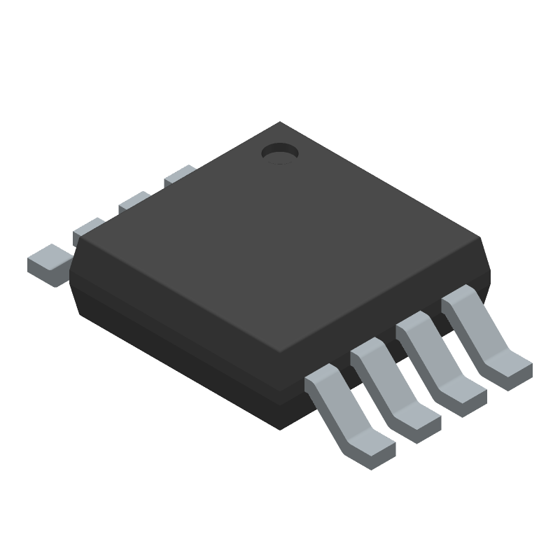
3D Model
Available Download Formats
By downloading CAD models, you agree to our Terms & Conditions and Privacy Policy
D Flip-Flop, LVC/LCX/Z Series, 1-Func, Positive Edge Triggered, 1-Bit, Complementary Output, CMOS, PDSO8
Tip: Data for a part may vary between manufacturers. You can filter for manufacturers on the top of the page next to the part image and part number.
74LVC1G74DP by Nexperia is an FF/Latch.
FF/Latches are under the broader part category of Logic Components.
Digital logic governs the behavior of signals in electronic circuits, enabling complex decisions based on simple binary inputs (yes/no). Logic components perform operations from these signals. Read more about Logic Components on our Logic part category page.
By downloading CAD models, you agree to our Terms & Conditions and Privacy Policy
|
|
74LVC1G74DP
Nexperia
Buy Now
Datasheet
|
Compare Parts:
74LVC1G74DP
Nexperia
D Flip-Flop, LVC/LCX/Z Series, 1-Func, Positive Edge Triggered, 1-Bit, Complementary Output, CMOS, PDSO8
|
| Rohs Code | Yes | |
| Part Life Cycle Code | Active | |
| Ihs Manufacturer | NEXPERIA | |
| Reach Compliance Code | compliant | |
| HTS Code | 8542.39.00.01 | |
| Samacsys Manufacturer | Nexperia | |
| Family | LVC/LCX/Z | |
| JESD-30 Code | S-PDSO-G8 | |
| JESD-609 Code | e4 | |
| Length | 3 mm | |
| Logic IC Type | D FLIP-FLOP | |
| Moisture Sensitivity Level | 1 | |
| Number of Functions | 1 | |
| Number of Terminals | 8 | |
| Operating Temperature-Max | 125 °C | |
| Operating Temperature-Min | -40 °C | |
| Output Polarity | COMPLEMENTARY | |
| Package Body Material | PLASTIC/EPOXY | |
| Package Code | TSSOP | |
| Package Shape | SQUARE | |
| Package Style | SMALL OUTLINE, THIN PROFILE, SHRINK PITCH | |
| Peak Reflow Temperature (Cel) | 260 | |
| Propagation Delay (tpd) | 13.4 ns | |
| Qualification Status | Not Qualified | |
| Seated Height-Max | 1.1 mm | |
| Supply Voltage-Max (Vsup) | 5.5 V | |
| Supply Voltage-Min (Vsup) | 1.65 V | |
| Supply Voltage-Nom (Vsup) | 1.8 V | |
| Surface Mount | YES | |
| Technology | CMOS | |
| Temperature Grade | AUTOMOTIVE | |
| Terminal Finish | NICKEL PALLADIUM GOLD SILVER | |
| Terminal Form | GULL WING | |
| Terminal Pitch | 0.65 mm | |
| Terminal Position | DUAL | |
| Time@Peak Reflow Temperature-Max (s) | 30 | |
| Trigger Type | POSITIVE EDGE | |
| Width | 3 mm | |
| fmax-Min | 200 MHz |
This table gives cross-reference parts and alternative options found for 74LVC1G74DP. The Form Fit Function (FFF) tab will give you the options that are more likely to serve as direct pin-to-pin alternates or drop-in parts. The Functional Equivalents tab will give you options that are likely to match the same function of 74LVC1G74DP, but it may not fit your design. Always verify details of parts you are evaluating, as these parts are offered as suggestions for what you are looking for and are not guaranteed.
| Part Number | Manufacturer | Composite Price | Description | Compare |
|---|---|---|---|---|
| 74LVC1G74DP | Philips Semiconductors | Check for Price | D Flip-Flop, 1-Func, Positive Edge Triggered, CMOS, PDSO8 | 74LVC1G74DP vs 74LVC1G74DP |
The maximum operating frequency of the 74LVC1G74DP is typically around 100 MHz, but it can vary depending on the specific application and operating conditions.
To ensure signal integrity, it's recommended to use a low-impedance PCB design, minimize trace lengths, and use termination resistors if necessary. Additionally, consider using a signal integrity analysis tool to simulate and optimize your design.
Yes, the 74LVC1G74DP can be used in a 3.3V system, but the output voltage will be limited to around 3.1V due to the device's voltage drop. This may affect the noise margin and signal integrity in some applications.
The 74LVC1G74DP is designed to handle power-up and power-down sequencing without any specific requirements. However, it's recommended to follow the power-up and power-down sequencing guidelines for the specific system to ensure reliable operation.
To minimize EMI and noise, it's recommended to follow good PCB design practices, such as keeping the device close to the power supply, using a solid ground plane, and minimizing trace lengths and loops. Additionally, consider using shielding and filtering components if necessary.