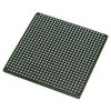
Part Details for 5CSEBA6U23I7N by Altera Corporation
Results Overview of 5CSEBA6U23I7N by Altera Corporation
- Distributor Offerings: (2 listings)
- Number of FFF Equivalents: (0 replacements)
- CAD Models: (Request Part)
- Number of Functional Equivalents: (1 option)
- Part Data Attributes: (Available)
- Reference Designs: (Not Available)
Tip: Data for a part may vary between manufacturers. You can filter for manufacturers on the top of the page next to the part image and part number.
5CSEBA6U23I7N Information
5CSEBA6U23I7N by Altera Corporation is a Field Programmable Gate Array.
Field Programmable Gate Arrays are under the broader part category of Programmable Logic Devices.
Programmable Logic Devices (PLDs) are reconfigurable digital components that can be customized for different applications, offering flexibility and improved performance over fixed logic devices. Read more about Programmable Logic Devices on our Programmable Logic part category page.
Price & Stock for 5CSEBA6U23I7N
| Part # | Distributor | Description | Stock | Price | Buy | |
|---|---|---|---|---|---|---|
|
DISTI #
544-3307-ND
|
DigiKey | IC SOC CORTEX-A9 800MHZ 672UBGA Min Qty: 1 Lead time: 12 Weeks Container: Tray |
45 In Stock |
|
$348.0300 | Buy Now |
|
DISTI #
989-5CSEBA6U23I7N
|
Mouser Electronics | SoC FPGA RoHS: Compliant | 192 |
|
$348.0300 | Buy Now |
Part Details for 5CSEBA6U23I7N
5CSEBA6U23I7N CAD Models
5CSEBA6U23I7N Part Data Attributes
|
|
5CSEBA6U23I7N
Altera Corporation
Buy Now
Datasheet
|
Compare Parts:
5CSEBA6U23I7N
Altera Corporation
Field Programmable Gate Array, 110000-Cell, CMOS, PBGA672, ROHS COMPLIANT, UBGA-672
|
| Rohs Code | Yes | |
| Part Life Cycle Code | Transferred | |
| Ihs Manufacturer | ALTERA CORP | |
| Part Package Code | BGA | |
| Package Description | ROHS COMPLIANT, UBGA-672 | |
| Pin Count | 672 | |
| Reach Compliance Code | compliant | |
| HTS Code | 8542.39.00.01 | |
| JESD-30 Code | S-PBGA-B672 | |
| Length | 23 mm | |
| Number of Inputs | 145 | |
| Number of Logic Cells | 110000 | |
| Number of Outputs | 145 | |
| Number of Terminals | 672 | |
| Package Body Material | PLASTIC/EPOXY | |
| Package Code | FBGA | |
| Package Equivalence Code | BGA672,28X28,32 | |
| Package Shape | SQUARE | |
| Package Style | GRID ARRAY, FINE PITCH | |
| Peak Reflow Temperature (Cel) | NOT SPECIFIED | |
| Programmable Logic Type | FIELD PROGRAMMABLE GATE ARRAY | |
| Qualification Status | Not Qualified | |
| Seated Height-Max | 1.85 mm | |
| Supply Voltage-Max | 1.13 V | |
| Supply Voltage-Min | 1.07 V | |
| Supply Voltage-Nom | 1.1 V | |
| Surface Mount | YES | |
| Technology | CMOS | |
| Terminal Form | BALL | |
| Terminal Pitch | 0.8 mm | |
| Terminal Position | BOTTOM | |
| Time@Peak Reflow Temperature-Max (s) | NOT SPECIFIED | |
| Width | 23 mm |
Alternate Parts for 5CSEBA6U23I7N
This table gives cross-reference parts and alternative options found for 5CSEBA6U23I7N. The Form Fit Function (FFF) tab will give you the options that are more likely to serve as direct pin-to-pin alternates or drop-in parts. The Functional Equivalents tab will give you options that are likely to match the same function of 5CSEBA6U23I7N, but it may not fit your design. Always verify details of parts you are evaluating, as these parts are offered as suggestions for what you are looking for and are not guaranteed.
| Part Number | Manufacturer | Composite Price | Description | Compare |
|---|---|---|---|---|
| 5CSEBA6U23I7N | Intel Corporation | Check for Price | Field Programmable Gate Array, 110000-Cell, CMOS, PBGA672, ROHS COMPLIANT, UBGA-672 | 5CSEBA6U23I7N vs 5CSEBA6U23I7N |
5CSEBA6U23I7N Frequently Asked Questions (FAQ)
-
Altera recommends a multi-layer PCB with a solid ground plane, and using differential pairs for high-speed signals. Additionally, it's essential to follow the guidelines for signal routing, decoupling, and power distribution outlined in the Altera FPGA PCB Design Guidelines document.
-
To optimize power consumption, use the PowerPlay Early Power Estimator (EPE) tool to estimate power consumption early in the design cycle. Implement power-saving techniques such as clock gating, voltage scaling, and dynamic voltage and frequency scaling. Also, consider using the Intel FPGA Power Director tool to analyze and optimize power consumption.
-
Implement a secure boot process using the Altera FPGA's built-in security features, such as the Secure Boot and Anti-Tamper (SBAT) feature. Use encryption and secure key storage, and consider implementing a secure firmware update mechanism. Additionally, follow the guidelines outlined in the Altera FPGA Security Handbook.
-
Use the Altera FPGA's built-in transceiver calibration and adaptation features to ensure reliable data transmission. Implement error correction mechanisms, such as CRC and ECC, and consider using a redundant transmission scheme. Additionally, follow the guidelines for transceiver signal integrity and PCB layout outlined in the Altera FPGA Transceiver User Guide.
-
The 5CSEBA6U23I7N FPGA has a maximum junction temperature of 100°C. Ensure good airflow around the device, and consider using a heat sink or thermal interface material to dissipate heat. Monitor the device's temperature using the on-chip thermal sensor and implement thermal throttling or shutdown mechanisms to prevent overheating.
