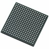
Part Details for 5CEBA4U15C7N by Altera Corporation
Results Overview of 5CEBA4U15C7N by Altera Corporation
- Distributor Offerings: (5 listings)
- Number of FFF Equivalents: (0 replacements)
- CAD Models: (Request Part)
- Number of Functional Equivalents: (0 options)
- Part Data Attributes: (Available)
- Reference Designs: (Not Available)
Tip: Data for a part may vary between manufacturers. You can filter for manufacturers on the top of the page next to the part image and part number.
5CEBA4U15C7N Information
5CEBA4U15C7N by Altera Corporation is a Field Programmable Gate Array.
Field Programmable Gate Arrays are under the broader part category of Programmable Logic Devices.
Programmable Logic Devices (PLDs) are reconfigurable digital components that can be customized for different applications, offering flexibility and improved performance over fixed logic devices. Read more about Programmable Logic Devices on our Programmable Logic part category page.
Price & Stock for 5CEBA4U15C7N
| Part # | Distributor | Description | Stock | Price | Buy | |
|---|---|---|---|---|---|---|
|
DISTI #
544-3223-ND
|
DigiKey | IC FPGA 176 I/O 324UBGA Min Qty: 1 Lead time: 12 Weeks Container: Tray |
280 In Stock |
|
$100.0600 | Buy Now |
|
DISTI #
989-5CEBA4U15C7N
|
Mouser Electronics | FPGA - Field Programmable Gate Array RoHS: Compliant | 0 |
|
$100.0600 | Order Now |
|
DISTI #
E54:1762_05927538
|
Arrow Electronics | FPGA Cyclone® V E Family 49000 Cells 28nm Technology 1.1V 324-Pin UBGA RoHS: Compliant Min Qty: 119 Package Multiple: 119 Lead time: 12 Weeks Date Code: 2437 | Europe - 13566 |
|
$97.0500 | Buy Now |
|
DISTI #
84990621
|
Verical | FPGA Cyclone® V E Family 49000 Cells 28nm Technology 1.1V 324-Pin UBGA RoHS: Compliant Min Qty: 119 Package Multiple: 119 Date Code: 2437 | Americas - 13566 |
|
$97.0500 | Buy Now |
|
|
Vyrian | Programmable ICs | 8962 |
|
RFQ |
Part Details for 5CEBA4U15C7N
5CEBA4U15C7N CAD Models
5CEBA4U15C7N Part Data Attributes
|
|
5CEBA4U15C7N
Altera Corporation
Buy Now
Datasheet
|
Compare Parts:
5CEBA4U15C7N
Altera Corporation
Field Programmable Gate Array, PBGA324, 15 MM, ROHS COMPLIANT, UBGA-324
|
| Pbfree Code | Yes | |
| Rohs Code | Yes | |
| Part Life Cycle Code | Transferred | |
| Ihs Manufacturer | ALTERA CORP | |
| Part Package Code | BGA | |
| Package Description | 15 MM, ROHS COMPLIANT, UBGA-324 | |
| Pin Count | 324 | |
| Reach Compliance Code | compliant | |
| HTS Code | 8542.39.00.01 | |
| JESD-30 Code | S-PBGA-B324 | |
| JESD-609 Code | e1 | |
| Length | 15 mm | |
| Moisture Sensitivity Level | 3 | |
| Number of Terminals | 324 | |
| Operating Temperature-Max | 85 °C | |
| Operating Temperature-Min | ||
| Package Body Material | PLASTIC/EPOXY | |
| Package Code | LFBGA | |
| Package Equivalence Code | BGA324,18X18,32 | |
| Package Shape | SQUARE | |
| Package Style | GRID ARRAY, LOW PROFILE, FINE PITCH | |
| Programmable Logic Type | FIELD PROGRAMMABLE GATE ARRAY | |
| Seated Height-Max | 1.5 mm | |
| Supply Voltage-Max | 1.13 V | |
| Supply Voltage-Min | 1.07 V | |
| Supply Voltage-Nom | 1.1 V | |
| Surface Mount | YES | |
| Temperature Grade | OTHER | |
| Terminal Finish | TIN SILVER COPPER | |
| Terminal Form | BALL | |
| Terminal Pitch | 0.8 mm | |
| Terminal Position | BOTTOM | |
| Width | 15 mm |
5CEBA4U15C7N Frequently Asked Questions (FAQ)
-
The recommended power-up sequence is to apply power to the core voltage (VCC) first, followed by the auxiliary voltage (VCCAUX) and then the input/output voltage (VCCIO). This ensures proper device operation and prevents damage.
-
To implement a reliable clock tree, use the FPGA's dedicated clock networks (GCLK) and follow Altera's guidelines for clock domain crossing, clock skew management, and clock tree synthesis.
-
To manage thermal issues, ensure good airflow around the device, use thermal interfaces (e.g., heat sinks, thermal tape) if necessary, and follow Altera's guidelines for thermal design and power estimation.
-
Optimize power consumption by using the FPGA's power-saving features (e.g., clock gating, power gating), reducing switching activity, and using low-power modes (e.g., sleep mode) when possible.
-
For signal integrity, follow Altera's guidelines for PCB design, use controlled impedance traces, and minimize signal reflections. Also, consider using signal termination and impedance matching techniques.
