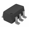
Part Details for 2N7002BKS by NXP Semiconductors
Results Overview of 2N7002BKS by NXP Semiconductors
- Distributor Offerings: (4 listings)
- Number of FFF Equivalents: (0 replacements)
- CAD Models: (Request Part)
- Number of Functional Equivalents: (0 options)
- Part Data Attributes: (Available)
- Reference Designs: (Not Available)
Tip: Data for a part may vary between manufacturers. You can filter for manufacturers on the top of the page next to the part image and part number.
2N7002BKS Information
2N7002BKS by NXP Semiconductors is a Small Signal Field-Effect Transistor.
Small Signal Field-Effect Transistors are under the broader part category of Transistors.
A transistor is a small semiconductor device used to amplify, control, or create electrical signals. When selecting a transistor, factors such as voltage, current rating, gain, and power dissipation must be considered, with common types. Read more about Transistors on our Transistors part category page.
Price & Stock for 2N7002BKS
| Part # | Distributor | Description | Stock | Price | Buy | |
|---|---|---|---|---|---|---|
|
|
ComSIT USA | AVAILABLE EU | 1500 |
|
RFQ | |
|
|
ComSIT USA | 60 V, 300 MILLI AMP DUAL N-CHANNEL TRENCH MOSFET Small Signal Field-Effect Transistor, 0.3A I(D), 60V, 2-Element, N-Channel, Silicon, Metal-oxide Semiconductor FET ECCN: EAR99 RoHS: Compliant |
|
|
RFQ | |
|
|
Vyrian | Transistors | 1636 |
|
RFQ | |
|
|
Win Source Electronics | 60 V, 300 mA dual N-channel Trench MOSFET | 120000 |
|
$0.0424 / $0.0547 | Buy Now |
Part Details for 2N7002BKS
2N7002BKS CAD Models
2N7002BKS Part Data Attributes
|
|
2N7002BKS
NXP Semiconductors
Buy Now
Datasheet
|
Compare Parts:
2N7002BKS
NXP Semiconductors
300mA, 60V, 2 CHANNEL, N-CHANNEL, Si, SMALL SIGNAL, MOSFET, PLASTIC, SC-88, 6 PIN
|
| Rohs Code | Yes | |
| Part Life Cycle Code | Transferred | |
| Ihs Manufacturer | NXP SEMICONDUCTORS | |
| Part Package Code | SC-88 | |
| Package Description | PLASTIC, SC-88, 6 PIN | |
| Pin Count | 6 | |
| Reach Compliance Code | unknown | |
| ECCN Code | EAR99 | |
| Additional Feature | ESD PROTECTION, LOGIC LEVEL COMPATIBLE | |
| Configuration | SEPARATE, 2 ELEMENTS WITH BUILT-IN DIODE | |
| DS Breakdown Voltage-Min | 60 V | |
| Drain Current-Max (ID) | 0.3 A | |
| Drain-source On Resistance-Max | 1.6 Ω | |
| FET Technology | METAL-OXIDE SEMICONDUCTOR | |
| JESD-30 Code | R-PDSO-G6 | |
| JESD-609 Code | e3 | |
| Moisture Sensitivity Level | 1 | |
| Number of Elements | 2 | |
| Number of Terminals | 6 | |
| Operating Mode | ENHANCEMENT MODE | |
| Operating Temperature-Max | 150 °C | |
| Operating Temperature-Min | -55 °C | |
| Package Body Material | PLASTIC/EPOXY | |
| Package Shape | RECTANGULAR | |
| Package Style | SMALL OUTLINE | |
| Peak Reflow Temperature (Cel) | NOT SPECIFIED | |
| Polarity/Channel Type | N-CHANNEL | |
| Qualification Status | Not Qualified | |
| Surface Mount | YES | |
| Terminal Finish | Tin (Sn) | |
| Terminal Form | GULL WING | |
| Terminal Position | DUAL | |
| Time@Peak Reflow Temperature-Max (s) | NOT SPECIFIED | |
| Transistor Application | SWITCHING | |
| Transistor Element Material | SILICON |
2N7002BKS Frequently Asked Questions (FAQ)
-
The maximum operating temperature range for the 2N7002BKS is -55°C to 150°C, as specified in the datasheet. However, it's recommended to operate the device within a temperature range of -40°C to 125°C for optimal performance and reliability.
-
To ensure the 2N7002BKS is fully turned on, the gate-source voltage (Vgs) should be at least 4.5V, and the drain-source voltage (Vds) should be within the specified range. Additionally, the gate current (Ig) should be limited to the recommended maximum value to prevent overheating.
-
The maximum current rating for the 2N7002BKS is 500mA, as specified in the datasheet. However, it's recommended to operate the device within a current range of 100mA to 300mA for optimal performance and reliability.
-
To protect the 2N7002BKS from ESD, it's recommended to handle the device with anti-static precautions, such as using an anti-static wrist strap or mat. Additionally, the device should be stored in an anti-static package or bag when not in use.
-
The recommended PCB layout for the 2N7002BKS involves keeping the drain and source pins as close as possible to minimize inductance and reduce electromagnetic interference (EMI). Additionally, the gate pin should be connected to a low-impedance source to minimize ringing and oscillations.
