-
Part Symbol
-
Footprint
-
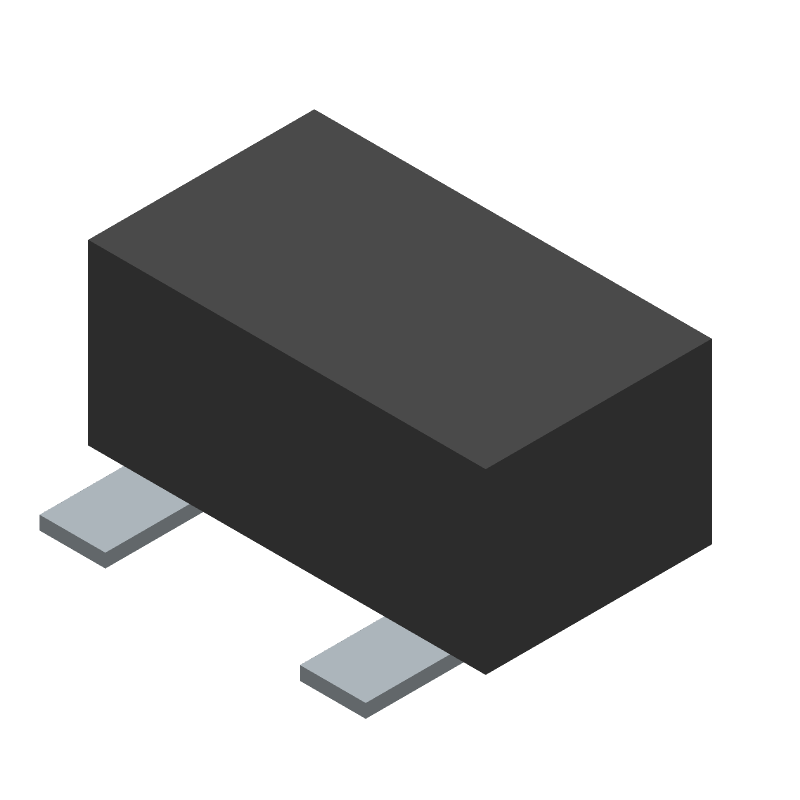
3D Model
Available Download Formats
By downloading CAD models, you agree to our Terms & Conditions and Privacy Policy

RF Small Signal Bipolar Transistor, 0.05A I(C), 1-Element, Very High Frequency Band, Silicon, NPN, SMT3, SC-59, 3 PIN
Tip: Data for a part may vary between manufacturers. You can filter for manufacturers on the top of the page next to the part image and part number.
2SC3837KT146N by ROHM Semiconductor is an RF Small Signal Bipolar Transistor.
RF Small Signal Bipolar Transistors are under the broader part category of Transistors.
A transistor is a small semiconductor device used to amplify, control, or create electrical signals. When selecting a transistor, factors such as voltage, current rating, gain, and power dissipation must be considered, with common types. Read more about Transistors on our Transistors part category page.
| Part # | Distributor | Description | Stock | Price | Buy | |
|---|---|---|---|---|---|---|
|
DISTI #
846-2SC3837KT146NCT-ND
|
DigiKey | RF TRANS NPN 20V 1.5GHZ SMT3 Min Qty: 1 Lead time: 18 Weeks Container: Digi-Reel®, Tape & Reel (TR), Cut Tape (CT) |
2961 In Stock |
|
$0.0912 / $0.5700 | Buy Now |
|
DISTI #
755-2SC3837KT146N
|
Mouser Electronics | Bipolar Transistors - BJT NPN 20V 50MA RoHS: Compliant | 920 |
|
$0.0940 / $0.4900 | Buy Now |
|
DISTI #
2SC3837KT146N
|
TME | Transistor: NPN, bipolar, 20V, 50mA, 200mW, SC59,SOT346 Min Qty: 5 | 2145 |
|
$0.0770 / $0.1630 | Buy Now |
|
DISTI #
2SC3837KT146N
|
Avnet Silica | Trans GP BJT NPN 20V 005A 3Pin SMT TR (Alt: 2SC3837KT146N) RoHS: Compliant Min Qty: 6000 Package Multiple: 3000 Lead time: 16 Weeks, 0 Days | Silica - 0 |
|
Buy Now |
By downloading CAD models, you agree to our Terms & Conditions and Privacy Policy
|
|
2SC3837KT146N
ROHM Semiconductor
Buy Now
Datasheet
|
Compare Parts:
2SC3837KT146N
ROHM Semiconductor
RF Small Signal Bipolar Transistor, 0.05A I(C), 1-Element, Very High Frequency Band, Silicon, NPN, SMT3, SC-59, 3 PIN
|
| Pbfree Code | Yes | |
| Rohs Code | Yes | |
| Part Life Cycle Code | End Of Life | |
| Ihs Manufacturer | ROHM CO LTD | |
| Part Package Code | SC-59 | |
| Package Description | SMT3, SC-59, 3 PIN | |
| Pin Count | 3 | |
| Reach Compliance Code | compliant | |
| ECCN Code | EAR99 | |
| Samacsys Manufacturer | ROHM Semiconductor | |
| Collector Current-Max (IC) | 0.05 A | |
| Collector-Base Capacitance-Max | 1.5 pF | |
| Collector-Emitter Voltage-Max | 20 V | |
| Configuration | SINGLE | |
| DC Current Gain-Min (hFE) | 56 | |
| Highest Frequency Band | VERY HIGH FREQUENCY BAND | |
| JESD-30 Code | R-PDSO-G3 | |
| JESD-609 Code | e1 | |
| Number of Elements | 1 | |
| Number of Terminals | 3 | |
| Operating Temperature-Max | 150 °C | |
| Package Body Material | PLASTIC/EPOXY | |
| Package Shape | RECTANGULAR | |
| Package Style | SMALL OUTLINE | |
| Polarity/Channel Type | NPN | |
| Power Dissipation Ambient-Max | 0.2 W | |
| Power Dissipation-Max (Abs) | 0.2 W | |
| Qualification Status | Not Qualified | |
| Surface Mount | YES | |
| Terminal Finish | TIN SILVER COPPER | |
| Terminal Form | GULL WING | |
| Terminal Position | DUAL | |
| Transistor Application | AMPLIFIER | |
| Transistor Element Material | SILICON | |
| Transition Frequency-Nom (fT) | 1500 MHz |
The recommended PCB footprint for the 2SC3837KT146N is a standard SOT-223 package with a minimum pad size of 1.5mm x 1.5mm and a thermal pad size of 2.5mm x 2.5mm.
To ensure reliable operation of the 2SC3837KT146N in high-temperature environments, it is recommended to follow proper thermal management practices, such as providing adequate heat sinking, using a thermal interface material, and keeping the junction temperature below the maximum rated value of 150°C.
The maximum safe operating area (SOA) for the 2SC3837KT146N is not explicitly stated in the datasheet, but it can be estimated based on the device's thermal and electrical characteristics. As a general rule, it is recommended to operate the device within the boundaries of the maximum ratings and to avoid operating conditions that may cause excessive heat generation or electrical stress.
Yes, the 2SC3837KT146N can be used in switching applications, but it is essential to ensure that the device is operated within its safe operating area and that the switching frequency is within the recommended range. The device's switching characteristics, such as rise and fall times, should also be considered to ensure reliable operation.
To handle ESD protection for the 2SC3837KT146N, it is recommended to follow proper ESD handling procedures, such as using ESD-safe workstations, wearing ESD-protective clothing, and using ESD-protective packaging. Additionally, it is recommended to use ESD protection devices, such as TVS diodes or ESD protection arrays, in the circuit design to protect the device from electrostatic discharge.