-
Part Symbol
-
Footprint
-
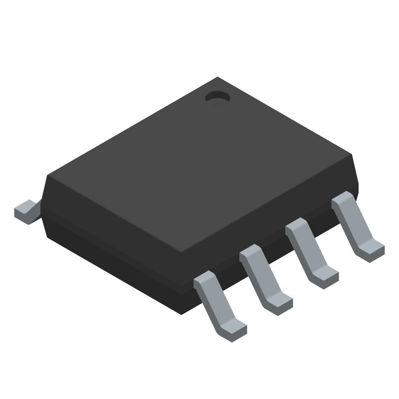
3D Model
Available Download Formats
By downloading CAD models, you agree to our Terms & Conditions and Privacy Policy
3.3V Zero Delay Clock Buffer, SOIC0/Reel
Tip: Data for a part may vary between manufacturers. You can filter for manufacturers on the top of the page next to the part image and part number.
2305A-1HDCG8 by Renesas Electronics Corporation is a Clock Driver.
Clock Drivers are under the broader part category of Logic Components.
Digital logic governs the behavior of signals in electronic circuits, enabling complex decisions based on simple binary inputs (yes/no). Logic components perform operations from these signals. Read more about Logic Components on our Logic part category page.
| Part # | Distributor | Description | Stock | Price | Buy | |
|---|---|---|---|---|---|---|
|
DISTI #
800-1277-1-ND
|
DigiKey | IC ZD BUFFER 8SOIC Min Qty: 1 Lead time: 12 Weeks Container: Digi-Reel®, Cut Tape (CT), Tape & Reel (TR) | Temporarily Out of Stock |
|
$0.4811 / $1.0600 | Buy Now |
|
DISTI #
2305A-1HDCG8
|
Avnet Americas | Clock Buffer, Zero Delay, 10 MHz to 133 MHz, 5 Outputs, 3 V to 3.6 V, 8 Pins, SOIC - Tape and Reel (Alt: 2305A-1HDCG8) RoHS: Compliant Min Qty: 3000 Package Multiple: 3000 Lead time: 12 Weeks, 0 Days Container: Reel | 0 |
|
$0.9100 | Buy Now |
|
DISTI #
972-2305A-1HDCG8
|
Mouser Electronics | Clock Buffer 3.3V PLL ZERO DELAY CLOCK BUFFER RoHS: Compliant | 0 |
|
$0.4870 / $1.0600 | Order Now |
|
DISTI #
2305A-1HDCG8
|
Avnet Silica | Clock Buffer Zero Delay 10 MHz to 133 MHz 5 Outputs 3 V to 36 V 8 Pins SOIC (Alt: 2305A-1HDCG8) RoHS: Compliant Min Qty: 3000 Package Multiple: 3000 Lead time: 13 Weeks, 0 Days | Silica - 0 |
|
Buy Now |
By downloading CAD models, you agree to our Terms & Conditions and Privacy Policy
|
|
2305A-1HDCG8
Renesas Electronics Corporation
Buy Now
Datasheet
|
Compare Parts:
2305A-1HDCG8
Renesas Electronics Corporation
3.3V Zero Delay Clock Buffer, SOIC0/Reel
|
| Pbfree Code | Yes | |
| Part Life Cycle Code | Active | |
| Ihs Manufacturer | RENESAS ELECTRONICS CORP | |
| Part Package Code | SOIC | |
| Package Description | SOP, SOP8,.25 | |
| Pin Count | 8 | |
| Manufacturer Package Code | DCG8 | |
| Reach Compliance Code | compliant | |
| HTS Code | 8542.39.00.01 | |
| Factory Lead Time | 12 Weeks | |
| Samacsys Manufacturer | Renesas Electronics | |
| Family | 2305 | |
| Input Conditioning | STANDARD | |
| JESD-30 Code | R-PDSO-G8 | |
| JESD-609 Code | e3 | |
| Logic IC Type | PLL BASED CLOCK DRIVER | |
| Max I(ol) | 0.012 A | |
| Moisture Sensitivity Level | 1 | |
| Number of Functions | 1 | |
| Number of Inverted Outputs | ||
| Number of Terminals | 8 | |
| Number of True Outputs | 4 | |
| Operating Temperature-Max | 70 °C | |
| Operating Temperature-Min | ||
| Output Characteristics | 3-STATE | |
| Package Body Material | PLASTIC/EPOXY | |
| Package Code | SOP | |
| Package Equivalence Code | SOP8,.25 | |
| Package Shape | RECTANGULAR | |
| Package Style | SMALL OUTLINE | |
| Packing Method | TR | |
| Peak Reflow Temperature (Cel) | 260 | |
| Qualification Status | Not Qualified | |
| Same Edge Skew-Max (tskwd) | 0.25 ns | |
| Supply Voltage-Max (Vsup) | 3.6 V | |
| Supply Voltage-Min (Vsup) | 3 V | |
| Supply Voltage-Nom (Vsup) | 3.3 V | |
| Surface Mount | YES | |
| Temperature Grade | COMMERCIAL | |
| Terminal Finish | MATTE TIN | |
| Terminal Form | GULL WING | |
| Terminal Pitch | 1.27 mm | |
| Terminal Position | DUAL | |
| Time@Peak Reflow Temperature-Max (s) | 30 | |
| fmax-Min | 133 MHz |
This table gives cross-reference parts and alternative options found for 2305A-1HDCG8. The Form Fit Function (FFF) tab will give you the options that are more likely to serve as direct pin-to-pin alternates or drop-in parts. The Functional Equivalents tab will give you options that are likely to match the same function of 2305A-1HDCG8, but it may not fit your design. Always verify details of parts you are evaluating, as these parts are offered as suggestions for what you are looking for and are not guaranteed.
| Part Number | Manufacturer | Composite Price | Description | Compare |
|---|---|---|---|---|
| 2305A-1DC8 | Integrated Device Technology Inc | Check for Price | PLL Based Clock Driver, 2305 Series, 4 True Output(s), 0 Inverted Output(s), PDSO8, SOIC-8 | 2305A-1HDCG8 vs 2305A-1DC8 |
| 2305A-1DCG | Renesas Electronics Corporation | Check for Price | 3.3V Zero Delay Clock Buffer, SOIC97/Tube | 2305A-1HDCG8 vs 2305A-1DCG |
| 2305A-1HDCGI | Integrated Device Technology Inc | Check for Price | SOIC-8, Tube | 2305A-1HDCG8 vs 2305A-1HDCGI |
| IDT2305A-1HDCG8 | Renesas Electronics Corporation | Check for Price | PLL Based Clock Driver, 2305 Series, 4 True Output(s), 0 Inverted Output(s), PDSO8 | 2305A-1HDCG8 vs IDT2305A-1HDCG8 |
| IDT2305A-1DCG8 | Renesas Electronics Corporation | Check for Price | PLL Based Clock Driver, 2305 Series, 4 True Output(s), 0 Inverted Output(s), PDSO8 | 2305A-1HDCG8 vs IDT2305A-1DCG8 |
| 2305A-1DCGI | Renesas Electronics Corporation | Check for Price | 3.3V Zero Delay Clock Buffer, SOIC97/Tube | 2305A-1HDCG8 vs 2305A-1DCGI |
| IDT2305A-1DCG | Renesas Electronics Corporation | Check for Price | PLL Based Clock Driver, 2305 Series, 4 True Output(s), 0 Inverted Output(s), PDSO8 | 2305A-1HDCG8 vs IDT2305A-1DCG |
Renesas provides a recommended PCB layout guide in their application note (R01AN3804EJ0100) which includes thermal vias, thermal pads, and heat sink recommendations to ensure optimal thermal performance.
Renesas recommends using an external overcurrent protection circuit, such as a current sense resistor and a comparator, to detect overcurrent conditions. The 2305A-1HDCG8 also has a built-in overcurrent detection feature, but it's not enabled by default and requires external resistors to set the detection threshold.
According to Renesas, the maximum allowed voltage on the VCC pin during power-up and power-down sequences is 6.5V. Exceeding this voltage may cause damage to the device.
Renesas provides EMC design guidelines in their application note (R01AN3804EJ0100) which include recommendations for PCB layout, component selection, and shielding to minimize electromagnetic interference.
The recommended operating temperature range for the 2305A-1HDCG8 is -40°C to 125°C. However, the device can operate up to 150°C with derating. It's essential to follow the thermal design guidelines to ensure reliable operation within the specified temperature range.