-
Part Symbol
-
Footprint
-
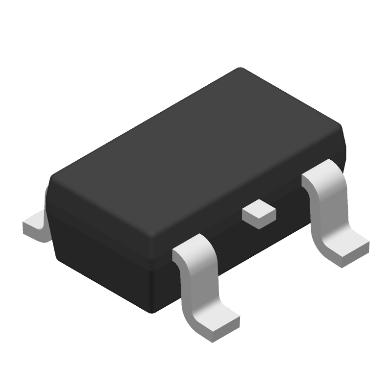
3D Model
Available Download Formats
By downloading CAD models, you agree to our Terms & Conditions and Privacy Policy

Automotive 5.5-V, 1:1 (SPST), 1-channel analog switch 5-SOT-23 -40 to 125
Tip: Data for a part may vary between manufacturers. You can filter for manufacturers on the top of the page next to the part image and part number.
1P1G66QDBVRQ1 by Texas Instruments is a Multiplexer or Switch.
Multiplexers or Switches are under the broader part category of Signal Circuits.
A signal is an electronic means of transmitting information, either as an analog signal with continuous values or a digital signal with discrete values. Signals are used in various systems and networks. Read more about Signal Circuits on our Signal Circuits part category page.
| Part # | Distributor | Description | Stock | Price | Buy | |
|---|---|---|---|---|---|---|
|
DISTI #
296-32005-1-ND
|
DigiKey | IC SWITCH SPST-NOX1 25OHM SOT23 Min Qty: 1 Lead time: 6 Weeks Container: Cut Tape (CT), Digi-Reel®, Tape & Reel (TR) |
5885 In Stock |
|
$0.1121 / $0.3000 | Buy Now |
|
DISTI #
595-1P1G66QDBVRQ1
|
Mouser Electronics | Analog Switch ICs Auto Cat Single Anal og Switch RoHS: Compliant | 3630 |
|
$0.1120 / $0.3000 | Buy Now |
|
DISTI #
1P1G66QDBVRQ1
|
TME | IC: analog switch, SPST, Ch: 1, SOT23-5, 1.65÷5.5VDC, reel,tape Min Qty: 1 | 0 |
|
$0.1820 / $0.4180 | RFQ |
|
|
LCSC | 35 1 SPST(SPST) SOT-23-5 Analog Switches Multiplexers ROHS | 585 |
|
$0.1155 / $0.1364 | Buy Now |
|
|
Win Source Electronics | IC SWITCH 1X1 SOT23-5 | 89000 |
|
$0.1557 / $0.2335 | Buy Now |
By downloading CAD models, you agree to our Terms & Conditions and Privacy Policy
|
|
1P1G66QDBVRQ1
Texas Instruments
Buy Now
Datasheet
|
Compare Parts:
1P1G66QDBVRQ1
Texas Instruments
Automotive 5.5-V, 1:1 (SPST), 1-channel analog switch 5-SOT-23 -40 to 125
|
| Pbfree Code | Yes | |
| Rohs Code | Yes | |
| Part Life Cycle Code | Active | |
| Ihs Manufacturer | TEXAS INSTRUMENTS INC | |
| Part Package Code | SOT-23 | |
| Pin Count | 5 | |
| Reach Compliance Code | compliant | |
| ECCN Code | EAR99 | |
| HTS Code | 8542.39.00.01 | |
| Samacsys Manufacturer | Texas Instruments | |
| Analog IC - Other Type | SPST | |
| Bandwidth-Nom | 300 MHz | |
| Input Voltage-Max | 5.5 V | |
| Input Voltage-Min | ||
| JESD-30 Code | R-PDSO-G5 | |
| JESD-609 Code | e4 | |
| Length | 2.9 mm | |
| Moisture Sensitivity Level | 1 | |
| Normal Position | NO | |
| Number of Channels | 1 | |
| Number of Functions | 1 | |
| Number of Terminals | 5 | |
| Off-state Isolation-Nom | 42 dB | |
| On-state Resistance-Max (Ron) | 30 Ω | |
| Operating Temperature-Max | 125 °C | |
| Operating Temperature-Min | -40 °C | |
| Output | COMMON OUTPUT | |
| Package Body Material | PLASTIC/EPOXY | |
| Package Code | LSSOP | |
| Package Equivalence Code | TSOP5/6,.11,37 | |
| Package Shape | RECTANGULAR | |
| Package Style | SMALL OUTLINE, LOW PROFILE, SHRINK PITCH | |
| Peak Reflow Temperature (Cel) | 260 | |
| Qualification Status | Not Qualified | |
| Screening Level | AEC-Q100 | |
| Seated Height-Max | 1.45 mm | |
| Signal Current-Max | 0.1 A | |
| Supply Current-Max (Isup) | 0.5 mA | |
| Supply Voltage-Max (Vsup) | 5.5 V | |
| Supply Voltage-Min (Vsup) | 1.65 V | |
| Supply Voltage-Nom (Vsup) | 2.3 V | |
| Surface Mount | YES | |
| Switch-off Time-Max | 8.9 ns | |
| Switch-on Time-Max | 9.5 ns | |
| Switching | BREAK-BEFORE-MAKE | |
| Technology | CMOS | |
| Temperature Grade | AUTOMOTIVE | |
| Terminal Finish | Nickel/Palladium/Gold (Ni/Pd/Au) | |
| Terminal Form | GULL WING | |
| Terminal Pitch | 0.95 mm | |
| Terminal Position | DUAL | |
| Time@Peak Reflow Temperature-Max (s) | 30 | |
| Width | 1.6 mm |
The maximum frequency of operation for the 1P1G66QDBVRQ1 is 100 MHz.
To ensure glitch-free operation, ensure that the select inputs (S0, S1) are changed only when the clock (CLK) is low. Additionally, the input signals should be synchronized with the clock signal.
The recommended power-up sequence is to apply VCC first, followed by the input signals, and then the clock signal. This ensures proper initialization of the device.
Yes, the 1P1G66QDBVRQ1 can be used as a demultiplexer by connecting the output channels to the desired output pins and configuring the select inputs accordingly.
To minimize power consumption, ensure that the input signals are properly terminated, and consider using a lower supply voltage (VCC) if possible. Additionally, consider using the shutdown mode (SD) to reduce power consumption when the device is not in use.